Polished Substrates
High quality, double side lapped and polished glass substrates (ex. Fused Silica Wafers) with extremely low surface roughness and flatness values.
Precision Polished Substrates
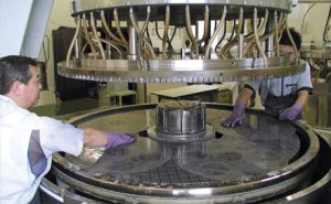
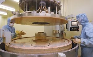
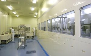
Ohara is a world class manufacturer of high quality double-side lapped and polished glass substrates. We supply precision polished glass, fused silica, optical glass, and glass-ceramic substrates for numerous applications including photomasks, DWDM filters, LCD’s, and glass mastering. Our Super Polished Substrates are cleaned using our 16 bath Megasonic Cleaning Unit and inspected in our Class 100 Clean Room. Our polished substrates are produced with extremely low surface roughness and flatness values, great for semiconductor packaging.
Ohara substrates are ideal for use in the temporary wafer bonding process. Our glass wafer carriers allow for semiconductor wafer thinning of various materials such as silicon, gallium arsenide, and others. We also provide laser marking for easy traceability.
Our high index wafers are ideal for low cost, high performance, consumer applications including AR/VR and other wearable devices.
Ohara’s GD-FHT™ is a finely polished glass disk used in the testing of magnetic recording heads designed for Hard Disk Drives. We supply three types of disks including Conventional, Low Waviness, and Super Low Waviness. These can be supplied with surface features such as anti-reflective coating. Conventional disks are well suited for fly height testing above 0.02 microns while Low and Super Low disks are used in lower fly heights around 0.01 microns. Ohara’s GD-FHT™ disks have better electrical properties and ESD protection when compared to competing materials. Combined with excellent mechanical strength, production yields can be significantly improved.
Ohara’s WMS™-15 glass-ceramic substrates enable manufacturers to produce leading edge DWDM and Gain-Flattening Filters and facilitate the production of filters with extremely low thermal wavelength drift and low insertion loss values. WMS™-15 has improved internal transmittance and exceptionally low surface roughness values.
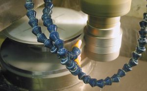
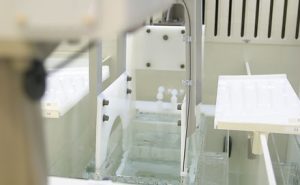
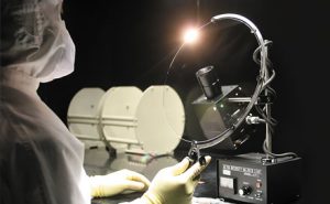
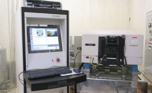
Photo Tour of Substrate Polishing