
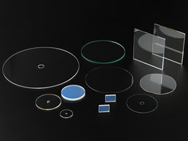
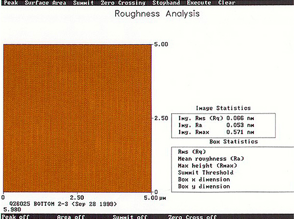
Our facility uses double-sided lapping and polishing machines to produce high quality plano substrates with extremely low surface roughness and flatness values. Some of the uses for our polished substrates include photomask substrates, TFT plates, phase masks and LCD’s.
Advantages
Ohara substrates are ideal for use in the temporary wafer bonding process. Our glass wafer carriers allow for semiconductor wafer thinning of various materials such as silicon, gallium arsenide, and others. We also provide laser marking for easy traceability.
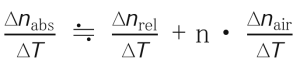
The temperature coefficient of refractive index of each glass type is measured as Δnabs/ΔT according to ISO 6760-1 and from this value the Δnrel/ΔT value normally used in optical design is calculated. The relationship between Δn abs/ΔT and Δn rel/ΔT is given by the following formula.
n :Refractive index of glass sample (in air, 25 ° C)
“Internal transmittance” refers to the spectral transmittance of the glass itself, not including reflection losses at the optical glass-air interface; it indicates the transparency of the glass. Most optical glasses absorb a substantial amount of light in the near-ultraviolet region. For some glasses, especially those with a high refractive index, this absorption range also extends into the visible range. This absorption is not only caused by the composition of the glass; it is also affected by impurities in the glass, and varies slightly from melt to melt.
The spectral transmittance (including reflection loss) is measured based on the JOGIS-17 standard at wavelengths from 280 nm to 2400 nm in a pair of glass samples with different distances through which transmitted light passes. Then, the internal transmittance 〔τ<sub>i</sub>(10 mm)〕 at a glass sample thickness of 10 mm is calculated from the measurement data.
CCI (Color Contribution Index) is an index for predicting how much the color of a photograph taken using a certain lens system changes compared to the original color, due to the spectral characteristics of the lens. It is indicated by a set of 3 numbers for blue (B) / green (G) / red (R). Ohara uses this index to predict how much the color will change as a single glass element. For the measurement method, refer to JIS B 7097 “How to express the color characteristics of a photographic lens by the ISO color characteristic index (ISO / CCI)”. The numbers shown are calculated using the sum of the values of the internal transmittance of the glass sample every 10 nm and the average color film weighted spectral sensitivity, described in JIS. For example, B / G / R of 0/3/5, is shown in Fig. 4 in trilinear coordinates.

Dispersion refers to the phenomenon arising from a variation in the refractive index depending on the wavelength. Here, nF-nC and nF’-nC’are displayed as the main dispersion. The Abbe number is an index of the magnitude of the variance and is also called the inverse dispersion rate. The larger the variance, the smaller the Abbe number.

The glass type data sheet indicates the dispersion, calculated from the refractive index to six decimal places . Abbe number is indicated to two decimal places, this is the result of the calculation from nd to six decimal places and the principal dispersion to six decimal places .
Two decimal places: This is the result of calculation from nd to six decimal places (with seven effective digits) and the principal dispersion to six decimal places (with four or more effective digits).
The temperature coefficient of the absolute refractive index of glass for wavelengths not listed in the data sheet can be calculated as a function of wavelength and temperature. Ohara uses the following equation.
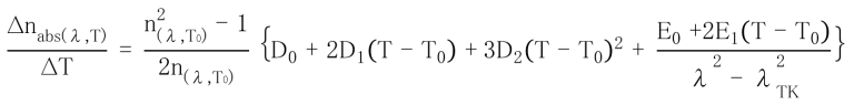
| n(λ,T0): | Refractive index at reference temperature |
| T0: | Reference temperature (°C) (Ohara defines this as 25°C) |
| T: | Target temperature (°C) |
| λ: | Vacuum wavelength (μm) |
| D0、D1、 D2、E0、 E1、λTK: | Constant (listed in the data sheet) |
To determine the temperature coefficient of the relative refractive index, refer to the equation given in the previous section, “Temperature coefficient of the refractive index”.
When light enters the glass, it slows down inversely proportional to the refractive index compared to in a vacuum or in air. The refractive index of optical glass is usually expressed as the speed ratio of light in the air to themedium (glass sample).
The refractive index is measured by sending a predetermined wavelength of light into the sample and measuring theminimum deviation angle of the emitted light bent by refraction, according to JIS B 7071-1. For the 20 spectral lines shown in the table below, numerical values are shown to five decimal places. The refractive indices (principal refractive indices) for d-line (587.56 nm) and e-line (546.07 nm) are also shown to six decimal places.
| Spectral Line Symbol | t | ||||
| Light Source | Hg | Hg | Hg | Hg | Hg |
| Wavelength (nm) | 2325.42 | 1970.09 | 1529.58 | 1128.64 | 1013.98 |
| Spectral Line Symbol | s | A′ | r | C | C′ |
| Light Source | Cs | K | He | H | Cd |
| Wavelength (nm) | 852.11 | 768.19 | 706.52 | 656.27 | 643.85 |
| Spectral Line Symbol | He-Ne | D | d | e | F |
| Light Source | レーザー | Na | He | Hg | H |
| Wavelength (nm) | 632.8 | 589.29 | 587.56 | 546.07 | 486.13 |
| Spectral Line Symbol | F′ | He-Cd | g | h | i |
| Light Source | Cd | レーザー | Hg | Hg | Hg |
| Wavelength (nm) | 479.99 | 441.57 | 435.835 | 404.656 | 365.015 |
The refractive index for wavelengths not listed in the data sheet can be calculated using the dispersion formula. The Sellmeier equation is used as a practical dispersion formula, as detailed below.
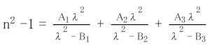
| n : | Refractive index to be calculated |
| λ : | Arbitrary wavelength (μm) |
| A1、A2、A3、B1、B2、B3 : | Constant (listed in the data sheet) |
Using this dispersion formula and the constants for each glass type, the refractive index of any wavelength in the standard measurement wavelength range (365 to 2325 nm) can be calculated with a calculation accuracy of ±5×10<sup>-6</sup>. However, for glass types for which the refractive indices for the entire standard measurement wavelength range are not listed in the data sheet, the applicable wavelength range of the dispersion formula is limited to the refractive index range listed in the data sheet.
Coloring refers to the degree of coloration of the optical glass and is determined by measuring the spectral transmittance, including reflection losses, for a glass sample with a thickness of 10 mm, according to JOGIS-02. From the spectral transmittance curve (Fig. 3), the wavelengths showing the transmittance of 80% and 5%, respectively, are rounded and displayed in 5 nm units. We use this rounding method: the range 0 nm to 2 nm counts as 0 nm, the range 3 nm to 7 nm counts as 5 nm, the range 8 nm to 10 nm counts as 10 nm . For example, if the wavelength with 80% transmittance is 403 nm and the wavelength with 5% transmittance is 357 nm, the coloring is shown as 405/355.

For glass types with a high refractive index, nd ≥ 1.84, the reflection loss is large, so the wavelength showing transmittance of 70 % is used, instead of 80 %, and the value is shown in paranethesis. For example, (415).
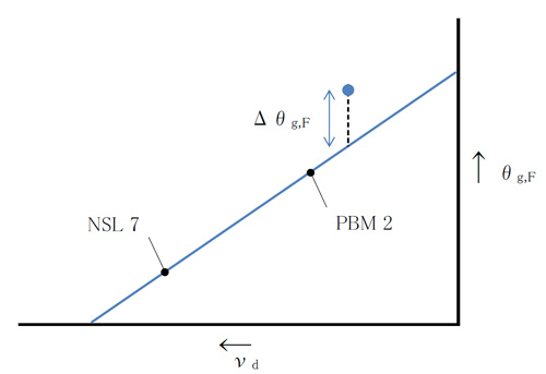
Although NSL 7 and PBM 2 are not currently produced by Ohara, the conventional NSL 7 and PBM 2 values (Table 2) are used as the reference values.
Reference Values
θc,t |
θC,A' |
θg,d |
θg,F |
θi,g |
vd |
|
NSL 7 |
0.8305 |
0.3492 |
1.2391 |
0.5436 |
1.2185 |
60.49 |
PBM 2 |
0.7168 |
0.3198 |
1.2894 |
0.5828 |
1.4214 |
36.26 |
>θg,F-νd図とΔθg,F