Polished Substrates
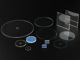
High quality, double side lapped and polished substrates (ex. Fused Silica Wafers) with extremely low surface roughness and flatness values.
Double Sided Precision Polished Substrates
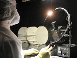
Our facility uses double-sided lapping and polishing machines to produce high quality plano substrates with extremely low surface roughness and flatness values. Some of the uses for our polished substrates include photomask substrates, TFT plates, phase masks and LCD’s.
Advantages
- Type of materials – quartz, fused silica, optical glasses, etc.
- Polished substrates available from 25 to 360 mm diameter
- 5″ and 6″ Sq. Photomask Substrates & custom sizes
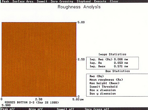
- RMS Values ~ 2 Angstroms (via AFM)
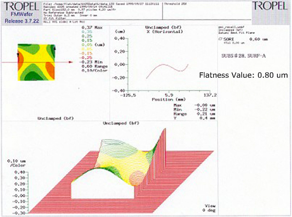
- Flatness Values ~ 1 micron (via Tropel Flatmaster)
- Substrates suitable for use at 248 nm
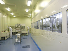
- Class 100 Clean Room and Megasonic Cleaning Unit
- Excellent Metrology Capabilities
Glass Wafer Carriers
Ohara substrates are ideal for use in the temporary wafer bonding process. Our glass wafer carriers allow for semiconductor wafer thinning of various materials such as silicon, gallium arsenide, and others. We also provide laser marking for easy traceability.
- Glass wafer carriers
- Temporary wafer bonding
- Laser marking
- Semiconductor wafer thinning
